
ASML Deep Dive: The Indispensable Enabler of Moore's Law
The company with a 100% monopoly on the future of technology.

For this month's deep dive, we are analyzing ASML, arguably the most critical company in the semiconductor supply chain. As we communicated earlier this year, we planned to publish 1-2 more deep dives on the semiconductor industry to expand our knowledge in the sector.
Following our February 2025 deep dive on AMD, we are now covering ASML, the company that produces the indispensable lithography machines used by every major chip manufacturer. In this write-up, we will provide a comprehensive overview of ASML, exploring its business model, technological monopoly, growth prospects, and valuation.
Contents:
Key Facts
Business Overview
Management
Industry
Financial Analysis
Competitive Advantages, Opportunities and Risks
Valuation
Conclusion
1. Key Facts
Description: ASML Holdings N.V. (ASML) is the global leader in lithography solutions, providing the critical Deep Ultraviolet (DUV) and Extreme Ultraviolet (EUV) machines that print circuit patterns onto silicon wafers. Its systems are indispensable to every major semiconductor fab, including TSMC, Intel, and Samsung and are essential for manufacturing the world's most advanced chips that power everything from smartphones to AI data centers.
Key Financials: From FY15 to TTM FY25, ASML achieved a revenue Compound Annual Growth Rate (CAGR) of 18.7% and operating income CAGR of 20.7%, reaching TTM FY25 revenue of €32.2 billion and operating income of €11.2 billion (34.8% operating margin). ASML holds €7.2 billion in cash and cash equivalents, compared to long term debt of €3.7 billion.
Price & Market Cap (as of 29 August 2025): Its market cap is €247 billion with a 52-week low of €508 and a 52-week high of €820, whereas it currently trades at €637.
Valuation: It trades at a LTM EV/EBITDA of 20x (5 Year average of 33.6x) and a LTM EV/Sales of 7.6x (5 Year average of 11.6x).
2. Business Overview
a. Lithography and its relation to Moore’s Law
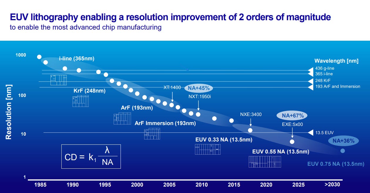
To understand ASML’s critical role, it is good to first get a high-level understanding on the process of lithography: projecting light onto a silicon wafer to print the circuit patterns for transistors. In essence, lithography enables “shrink”: the reduction of transistor size. The machine determines the smallest features that can be printed on a chip and, therefore, the number of transistors that can be packed into a given area (more transistors means more powerful and energy-efficient chips).
This capability is fundamentally tied to two factors: the wavelength of light the machine projects on the wafer and the Numerical Aperture (NA) of the system's optics. A shorter wavelength allows for finer patterns, while a higher NA which you can think of as the optics' (mirrors and lenses) ability to gather light and focus it precisely also enables the printing of smaller features.
Together, these advancements in lithography are the engine behind Moore's Law, the famous observation by Intel's co-founder Gordon Moore that the number of transistors on a chip double approximately every two years. For decades, this doubling has been a direct result of continuous improvements in lithography technology. While the pace of shrink has slowed as physical limits are approached, it is still the primary path forward for the industry. The ongoing advancements made by ASML are what make this continued progress possible, reinforcing lithography’s position as the key driver for reducing both the cost and energy consumption per transistor.
b. The Lithography Machine
The primary objective of lithography is to reduce the cost per transistor by enabling chipmakers to produce the highest number of good transistors possible on a single chip. To achieve this, ASML builds machines of unprecedented scale and complexity.
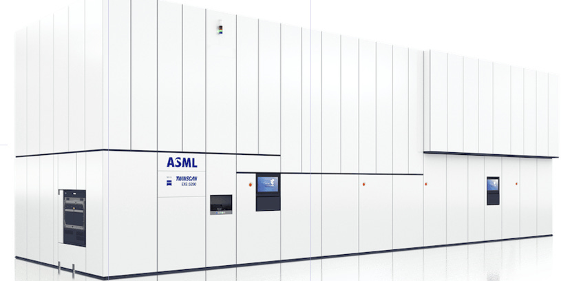
A single EUV system is about the size of a city bus, contains over 100,000 parts, and costs upwards of $200 million. This immense cost and complexity are why a lithography system represents the single largest equipment investment a chip factory makes.
Source: ASML
c. The ASML Story
In 1984, ASM Lithography (later ASML) was born as a joint venture between Philips and Advanced Semiconductor Materials International (ASMI). The technology that formed the company originated in Philips's own research labs, where scientists had developed a "wafer stepper" to give their internal chip division a competitive edge. Seeing its potential, Philips decided to spin off the division to sell the machines externally but, seeking to limit its financial exposure, partnered with ASMI.
The company’s early years were a struggle. Its first commercial product, the PAS 2000, was not a financial success, but it introduced an innovative alignment technology that would become a cornerstone of ASML's future systems. While an improved machine, the PAS 2400, helped secure AMD as the first external customer in 1987, ASML still struggled to win over industry leaders like Intel and IBM, who were reluctant to switch from the era's dominant players, Nikon and Canon. Faced with continued funding needs, ASMI withdrew from the venture in 1988. However, a strategic investment by Philips into a new Taiwanese foundry, TSMC, opened the door for ASML to land the client that would eventually become its biggest customer.
The PAS 5500 and Modular Design
The true turning point came in 1991 with the prototype of the PAS 5500, a machine that helped ASML finally gain IBM as a client. Its breakthrough was a revolutionary modular design, a first in the industry. While its vertically integrated Japanese competitors built everything themselves in a monolithic system, ASML outsourced the manufacturing of individual modules to specialized suppliers. This design allowed for machines to be upgraded without being fully replaced and enabled a more capital-efficient business model. The longevity of this approach is remarkable; a stunning 95% of all systems ASML has ever shipped are still in operation. The company explicitly designs its systems with a 20-year lifetime in mind, which not only benefits customers but also creates a significant and stable revenue stream from its service and upgrade business.
IPO and the SVG Acquisition
With the success of the PAS 5500, ASML became profitable by 1993 and held its IPO in 1995, separating from Philips. The journey was not a straight line, as the company's fortunes were tied to the volatile semiconductor cycles. During the dot-com bubble, sales peaked at €2.8 billion in 2000, only to fall by 41% the following year; the stock took nearly 12 years to recover its peak price.
However, during this downturn, ASML made a pivotal strategic move, acquiring the US-based Silicon Valley Group (SVG) for $1.6 billion in stock. The acquisition was a masterstroke that accomplished two goals: it secured Intel, SVG’s largest client, and it brought in the foundational licenses for a new, undeveloped, and highly ambitious technology—EUV. This bet on the future would ultimately cement ASML's monopoly decades later.
The DUV Wall and Immersion
For many years, DUV lithography was the industry standard, using light with a 193-nanometer wavelength to print circuits. By the early 2000s, however, the industry's relentless push for "shrink" meant that chip structures were becoming finer than what DUV light could physically resolve.
While ASML initially made advances by improving the resolution of its lenses (increasing the Numerical Aperture), a more fundamental solution was needed. In the meantime, ASML introduced a stroke of genius: immersion lithography. By placing a thin layer of water between the machine's lens and the silicon wafer, ASML was able to effectively shorten the DUV wavelength and print even smaller features. Introduced in 2004, immersion technology was a critical bridge that kept Moore's Law alive while the industry worked on the ultimate, far more complex solution.
Source: ASML Investor Day Presentation 2024
A Collaborative Bet on EUV
The long-term answer was Extreme Ultraviolet (EUV) lithography, a revolutionary technology using an incredibly short wavelength of just 13.5 nanometers. However, the challenge was immense; it would take nearly two decades and billions of dollars to commercialize the technology for high-volume manufacturing.
ASML did not have the funds to finance the entire EUV research program and acquire its key supplier, Cymer (the US company developing the EUV light source). Doing so would have meant shouldering the risk for the entire industry. In an unprecedented move in 2012, ASML persuaded its largest customers, Intel, Samsung, and TSMC, to co-fund the project. They collectively invested approximately €5 billion in ASML in exchange for a combined 25% stake, ensuring the technology that was essential for their own future roadmaps would become a reality.
This journey has culminated in ASML's current market dominance: today, the company is the world's only manufacturer of EUV machines, holding a 100% market share, while also commanding a strong majority share of 80%- 90% in the DUV market.
Today, these two technologies serve different market segments. DUV systems are the workhorses used to produce mature chips for applications like cars and appliances, while EUV is essential for the most advanced chips powering smartphones and AI data centers.
(For those interested in a deeper look at the company’s history, we highly recommend the book “Focus: The ASML Way” by Marc Hijink.)